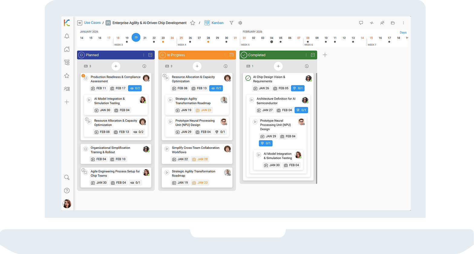
AI-Driven Semiconductor Design
Technology Sector
As robotics and automation continue to evolve, the transition to AI-enabled semiconductor design represents a critical strategic inflection point. High-performance chips must support real-time sensing, decision-making, and motor control. KanBo provides a structured, transparent, and agile platform that empowers engineering, design, and production teams to coordinate seamlessly, enabling faster innovation and greater efficiency in semiconductor R&D and fabrication.
Company’s Overview
Industry:
AI-Driven Semiconductor & Chip Design
Key Focus Areas:
AI chip architecture, advanced manufacturing, lifecycle efficiency
Size:
Globally integrated semiconductor company with R&D, design, and production operations
Challenges:
Complex R&D cycles, resource alignment, production delays, regulatory compliance
Stakeholder Perspective
Chief Technology Officer (CTO) of an AI Semiconductor Company
Realigning our semiconductor design toward AI architectures requires tight orchestration between innovation, engineering, and production. KanBo brings visibility and structure to our development lifecycle, allowing us to iterate faster, allocate resources effectively, and maintain compliance and performance standards across all phases.
Get started today with KanBo!
You can see KanBo in action by accessing our Sandbox demonstration environment.

How the Organization Uses KanBo
KanBo enables end-to-end coordination across AI semiconductor research, development, and production. With structured digital workspaces and collaborative tools, teams are empowered to innovate efficiently and bring AI-enabled chips to market faster.
I. R&D Strategy & Innovation Management
- Hierarchical Workspaces: Separate spaces for concept design, algorithm development, and prototyping.
- Mind Maps & Cards: Organize research milestones and project dependencies.
- Forecast Charts: Visualize R&D progress and allocate resources dynamically.
II. Task Execution & Production Workflow
- Card-Based Milestones: Manage fabrication checkpoints and quality gates.
- Workflow Automation: Reduce latency in design validation and production scaling.
- Dependency Tracking: Map sequential and parallel tasks across teams.
III. AI Model Integration & Testing
- Collaborative Spaces: Facilitate iterative model training and testing workflows.
- Performance Charts: Assess chip capabilities based on evolving algorithm outputs.
- Real-Time Feedback Loops: Engineer and validate neural processing units (NPUs).
IV. Resource Planning & Capacity Utilization
- Resource Modules: Allocate engineering time, compute infrastructure, and testing facilities.
- Work Schedule Management: Align specialist availability with project stages.
- Materials Tracking: Manage access to rare or critical chip fabrication resources.
V. Quality Assurance & Compliance Management
- QA Templates: Standardize defect analysis and validation protocols.
- Document Storage: Central repository for safety, compliance, and audit records.
- Regulatory Dashboards: Monitor industry standard adherence and updates.
VI. Strategic Insight & Executive Oversight
- Executive Dashboards: Track KPIs across the chip lifecycle.
- Scenario Planning Tools: Simulate market impact of technical changes.
- Secure Access Controls: Role-based views for leadership, engineering, and compliance.
Roadmap for Implementation
Planning and Setup
Pilot Phase
Pilot Evaluation
Full Rollout
Project Highlights
Pilot Duration:
6-month design and validation cycle
System Integrations:
Microsoft Teams, SharePoint, and proprietary semiconductor databases
Performance Improvements:
30% reduction in development latency, accelerated production cycles
Real-World Applications in KanBo
AI-Driven Chip Lifecycle Management
KanBo’s Card and Space structure enabled the team to track every NPU iteration, testing metric, and algorithm refinement with full traceability.
Supply Chain Coordination
Material shortages were mitigated by using KanBo’s integrated supply chain dashboards and alerts, reducing production risks.
Global Collaboration & IP Security
Hybrid deployment ensured secure on-premises IP protection while enabling remote collaboration across continents.
Benefits of Using KanBo in Semiconductor Development
Workflow Transparency
Structured tracking across all chip development stages
Optimized Resource Use
Efficient deployment of technical, operational, and physical resources
Data-Driven Insights
Predictive analytics and scenario planning for high-stakes innovation
End-to-End Collaboration
Unified communication across R&D, production, and executive leadership
Security and Installation Options
On-Premises & Government Cloud Deployment
Ensures compliance with national security regulations.
Role-Based Access Controls
Restrict sensitive investment data to authorized personnel.
Data Encryption & Audit Logging
Protects against cyber threats and ensures transparency.
KanBo – Work Coordination Platform
KanBo is a work coordination software designed to help self-organizing teams work smarter and faster. You can see KanBo in action by accessing our demonstration environment.
